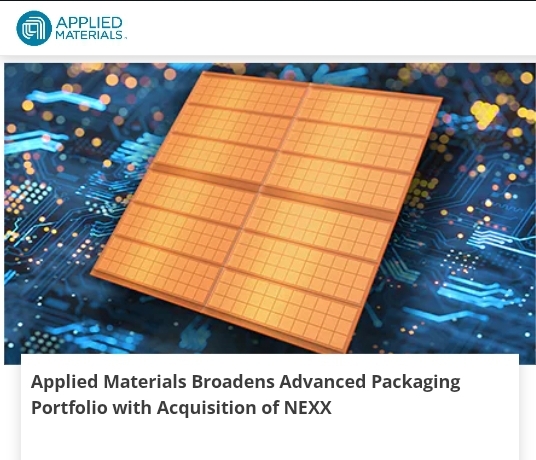
Applied Materials Elevates Advanced Packaging Portfolio for AI Scale
Applied Materials Elevates Advanced Packaging Portfolio in the AI Compute Era
The semiconductor industry is entering a decisive inflection point where performance is no longer dictated solely by transistor scaling. Applied Materials Elevates Advanced Packaging Portfolio through its acquisition of NEXX from ASMPT Limited—signaling a structural shift toward system-level innovation that directly impacts AI compute scalability, efficiency, and customer outcomes.
At a structural level, this move reframes packaging from a backend process into a primary performance lever. The deeper implication is clear: the future of AI infrastructure will be defined not just by chips, but by how those chips are integrated, interconnected, and scaled.
The AI Compute Pressure That Is Redefining Architecture
AI workloads are accelerating beyond the limits of traditional semiconductor design. Training large models and deploying inference at scale now require integrating multiple compute elements—GPUs, high-bandwidth memory (HBM), and I/O subsystems—into unified architectures.
This becomes critical when legacy 300mm wafer-based packaging approaches fail to deliver:
- Required interconnect density
- Thermal efficiency at scale
- Economical large-package production
The deeper implication is that the industry is transitioning from monolithic chips → chiplet-based systems, where packaging becomes the architecture itself.
From a CX standpoint, enterprise customers now expect:
- Faster AI model deployment cycles
- Predictable performance at scale
- Lower energy consumption per workload
This is where the shift occurs—customer experience is now directly tied to packaging innovation.
Why Applied Materials Elevates Advanced Packaging Portfolio Matters Now
“Having NEXX join Applied Materials complements our leadership in advanced packaging, particularly in panel processing – an area where we see tremendous opportunities for customer co-innovation and growth in the years ahead,” — Dr. Prabu Raja, President, Semiconductor Products Group, Applied Materials
Strategically, this acquisition is not about incremental capability expansion—it is about owning the integration layer of semiconductor manufacturing.
Old Model:
- Process-centric optimization
- Packaging as a downstream activity
New Model:
- System-level co-optimization
- Packaging as a primary value driver
Applied Materials Elevates Advanced Packaging Portfolio by integrating NEXX’s electrochemical deposition (ECD) capabilities into its broader ecosystem, enabling tighter coupling across lithography, deposition, and metrology systems.
This becomes critical when performance gains increasingly depend on how efficiently multiple chips communicate within a package.
Competitive Dynamics Are Shifting Beneath the Surface
The competitive battlefield in semiconductors is quietly moving from node scaling to packaging integration.
- Lam Research and Tokyo Electron remain strong in core process equipment but lack comparable integrated panel-level packaging ecosystems.
- TSMC and Intel are advancing packaging capabilities but rely on suppliers like Applied Materials for critical tooling.
- Emerging players are innovating in chiplet interconnects but lack manufacturing scale.
This is where the shift occurs:
From competing on individual tools → competing on integrated platforms.
By strengthening its panel-level packaging capabilities, Applied positions itself between infrastructure providers and system architects—effectively becoming a platform orchestrator.
The Technology Stack That Enables Scale and Efficiency
“NEXX’s products are already strong, and we intend to build on our success as part of Applied Materials with a continued focus on innovation, quality and excellent customer service,” — Jarek Pisera, President, ASMPT NEXX
At a technical level, the acquisition fills a critical gap in Applied’s portfolio.
Core Stack Now Includes:
- Digital Lithography
- Physical Vapor Deposition (PVD)
- Chemical Vapor Deposition (CVD)
- Etch Systems
- eBeam Metrology & Inspection
- Electrochemical Deposition (ECD) via NEXX
Orchestration Layer:
These technologies are not standalone—they must operate in tightly synchronized workflows to enable:
- Fine-pitch interconnect formation
- High-yield large-area processing
- Multi-chip integration at scale
Panel-Level Advantage:
Moving from wafer-based to panel-level substrates (up to 510×515 mm) enables:
- Larger chip footprints
- Increased throughput
- Lower cost per function
Operationally, this translates into faster production cycles and improved manufacturing efficiency—directly impacting time-to-market.
From Technology to Experience: The CX Translation
From a CX standpoint, the implications extend far beyond fabrication.
Customer Impact (Chipmakers & Hyperscalers)
- Faster deployment of AI infrastructure
- Improved performance-per-watt
- Greater design flexibility
Business Impact
- Reduced total cost of ownership (TCO)
- Accelerated innovation cycles
- Stronger competitive differentiation
System Impact
- Seamless chiplet integration
- Improved thermal management
- Higher reliability at scale
This becomes critical when enterprises demand predictable, scalable, and efficient compute experiences.
The deeper implication is that packaging innovation directly shapes end-user digital experiences—from AI applications to cloud services.
Maturity Signals and the Next Inflection Point
At a maturity level, the industry is transitioning toward system-orchestrated CX (Level 4).
- Integration across multiple process layers is becoming standard
- Performance optimization is shifting from component-level to system-level
However, gaps remain:
- Lack of standardization in chiplet ecosystems
- Interoperability challenges across vendors
This is where the next inflection point lies—whoever solves ecosystem integration at scale will define the next phase of semiconductor leadership.
Decision Intelligence: Build vs Buy vs Control
Applied’s decision to acquire rather than build internally reflects a clear strategic calculus.
Build
- High control
- Slow execution
- Significant R&D risk
Buy (Chosen Path)
- Rapid capability acquisition
- Faster time-to-market
- Integration complexity risk
Partner
- Flexible
- Limited control
The deeper implication is that control over advanced packaging capabilities is becoming synonymous with control over AI infrastructure value chains.
Industry-Wide Ripple Effects
This move is expected to reshape multiple dimensions of the semiconductor ecosystem:
Talent
Demand will surge for cross-domain expertise spanning materials science, systems engineering, and AI workloads.
Competition
The battleground shifts from process nodes → packaging platforms.
Ecosystem
Collaboration between equipment vendors, chipmakers, and system integrators will intensify.
Strategically, this indicates a transition toward platform-led semiconductor ecosystems, where integration capability defines leadership.
The Future: Packaging as the Core of AI Infrastructure
As AI systems grow in complexity, the industry will move toward:
- Larger and more complex chiplet architectures
- Higher-density interconnects
- Fully integrated system-level optimization
Applied Materials Elevates Advanced Packaging Portfolio not as an incremental expansion—but as a foundational repositioning to lead this transition.
This becomes critical when the next wave of AI innovation depends not just on compute power—but on how efficiently that power is packaged, connected, and delivered.
Final Takeaways: What This Really Changes
- Packaging is becoming the primary driver of semiconductor innovation
- AI demand is forcing a shift toward system-level integration
- Panel-level processing will redefine cost and scalability economics
- Tool vendors are evolving into platform orchestrators
- Applied Materials Elevates Advanced Packaging Portfolio to position itself at the center of this transformation
The deeper implication is unmistakable:
The future of semiconductors—and the experiences they enable—will be defined by integration, not just invention.
The post Applied Materials Elevates Advanced Packaging Portfolio for AI Scale appeared first on CX Quest.


추천 콘텐츠
In 3-6 Days, Bitcoin Enters Its Last Dip Before the Next Leg Higher – Watch This Level

200+ Firms Urge Senate to Enact CLARITY Act for Crypto Regulation

Gold continues to hit new highs. How to invest in gold in the crypto market?